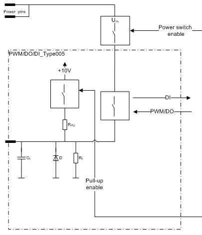
PWM/DO/DI_Type005
|

|
When using this type of pin, the related power switch must be switched on as well. See related power switches in section I/O List table's column named Group. Before the supply voltage can be connected to an output pin, the related power switch must be on. If the related power switch is off, the pin's input state is 1 (TRUE).
|
Output (PWM/DO)
-
This kind of pin is a current sourcing output with a pull-up selection
-
In other words, the pin connects the load to a positive supply voltage
-
When the pull-up is selected, it will affect two output pins (the pairs are indicated with upper case characters in the pin table's Group column in section Pinout Map).
-
This pull-up feature is for open load detection when the pin is used as an output.
-
These outputs have a switching element called a smart FET. It has integrated features to protect itself and also the external pin, wiring and actuator.
-
These outputs are capable of generating pulse width modulated (PWM) output signals.
-
When used as an output, the input feature indicates the output FET's state
|
|
It is recommended to use the function blocks in DigitalOutputDiagnostics library to protect and diagnose outputs when used as digital outputs. For more information, refer to Epec Programming and Libraries Manual.
|
Input (DI)
-
This pin can be used as a digital input (DI)
-
A pin of this type can also be used as an input by using the output state monitoring feature.
-
In this case, the output functionality of the pin must be kept in the off state.
-
It must be taken care in system design that the output unintentionally switching to on state causes no harm to the system.
-
This pin can be used also with NPN-type sensors – sensors with open collector/open drain.
Electrical characteristics
|
Symbol
|
Parameter
|
Conditions
|
Min
|
Max
|
Units
|
|
VLevel
|
Output voltage
|
Output Off, Pull-up selected, Unconnected pin
|
typ. 8,3
|
V
|
|
Io
|
Nominal Output Current
|
Output On
(Note 7)
|
0
|
4
|
A
|
|
Io-lim
|
Internal current limitation
|
Output On (Note 5, 9)
|
typ. 8
|
A
|
|
RPU
|
Pull-up Resistance
|
Selectable pull-up (off/10 V)
|
typ. 2,2
|
kΩ
|
|
fPWM
|
PWM Frequency
|
(Note 1)
|
10
|
3000
|
Hz
|
|
DutyPWM
|
PWM
Duty cycle
|
(Note 2, 10)
|
0 to 100
|
%
|
|
ResPWM
|
PWM Resolution
|
(Note 3)
|
0,1
|
%
|
|
Digital status input
|
|
RI
|
Input Resistance
|
Output Off, Pull-up resistor not selected
|
typ. 12
|
kΩ
|
|
VIH
|
Digital status input
High Voltage level
|
Output Off (Note6)
|
3,2
|
|
V
|
|
VIL
|
Digital status input
Input Low Voltage
|
Output Off
|
|
1,9
|
V
|
|
VI-range
|
Input voltage range
|
(Note 11)
|
-0,5
|
Uin + 0,2V
|
V
|
|
tI
|
Digital Status Input
Pulse Width
|
(Note 2, 4, 8)
|
> tC
|
ms
|
|
CI
|
Input pin capacitance
|
|
typ. 1
|
nF
|
Note 1: The frequency of a (PWM) Pulse Width Modulation is = 1 / Period
Note 2: The duty cycle is defined as the percentage of digital ‘high’ to digital ‘low’ signals present during a PWM period.
Note 3: The PWM resolution is defined as the maximum number of pulses that you can pack into a PWM period.
Note 4: tC denotes the software cycle time.
Note 5: Current limit for short circuit protection to protect cabling and to limit internal power dissipation.
Note 6: Exceeding the max value might cause damage to input.
Note 7: The maximum output current depends on the load, PWM frequency and temperature.
Note 8: The pulse width must be greater that the software cycle time. For example with 50/50 pulse ratio, the pulse frequency is 1 / (2*pulse width)
Note 9: When the limit is exceeded, the output voltage circuit starts to limit the current by switching the output voltage. The switching does not effect the application software
Note 10: When the frequency increases, the actual duty cycle may be bigger than the value that has been set.
Note 11: Overload conditions
Functional block diagram
|
|
Refer to section Connection Examples to see examples of how to connect external actuators or sensors when using this type of pin.
|