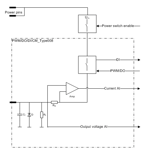
PWM/DO/DI/CM_Type008
|

|
When using this type of pin, the related power switch must be switched on as well. See related power switches in section I/O List table's column named Group. Before the supply voltage can be connected to an output pin, the related power switch must be on. If the related power switch is off, the pin's input state is 1 (TRUE).
|
Output (PWM/DO)
-
This type of pin is a current sourcing output with a current and voltage measurement features (the pin connects the load to a positive supply voltage through the shunt resistors).
-
These outputs have a switching element called a smart FET. It has integrated features to protect itself and also the external pin, wiring and actuator.
-
These outputs are capable of generating pulse width modulated (PWM) output signals.
-
When used as an output, the input feature indicates the output FET's state
|
|
The FET outputs are grouped into pairs:
-
The maximum continuous current for a single output in the pair is 2,5 A.
-
The maximum continuous current for the pair is 4 A.
The pairs are indicated with upper case characters in the pin table's Group column in section I/O List
|
|
|
It is recommended to use the function blocks in DigitalOutputDiagnostics library to protect and diagnose outputs when used as digital outputs. For more information, refer to Epec Programming and Libraries Manual.
|
Input (DI/AI)
-
In this case, the output functionality of the pin must be kept in the off state.
-
These pins may also be used as analog inputs (AI)
-
It must be taken care in system design that the output unintentionally switching to on state causes no harm to the system.
-
It’s highly recommended to use closed loop connections when the output pin is used as an input. By keeping this simple principle in mind, will help avoid problems later on.
Voltage measurement
-
When the pin is used as an output, the application can control the voltage with the voltage measurement feature
-
When the pin is used as an input, the application can measure the input voltage level
|

|
The measured voltage must not exceed the operating voltage!
|
Current measurement
-
When the pin is used as an output, the application can control the current with the current measurement feature
-
The firmware limits the maximum current to 2,5 A (when the current exceeds the value more than 200 ms, the output is switched off)
Electrical characteristics
|
Symbol
|
Parameter
|
Conditions
|
Min
|
Max
|
Units
|
|
RShunt
|
Shunt resistance
|
|
typ. 68
|
mΩ
|
|
Io-range
|
Nominal Current Measuring Range
|
|
0
|
3,5
|
A
|
|
fCut-Off
|
Cut-off frequency
|
Output current measuring
|
typ. 50
|
Hz
|
|
Iacc-zero
|
Offset error
|
Calculated 'worst case'
|
|
+/-0,9
|
%
|
|
|
+/-33,0
|
mA
|
|
Iacc-prop
|
Accuracy
Proportional factor
|
Calculated 'worst case'
|
|
+/-3,2
|
%
|
|
|
+/-117,7
|
mA (FS)
|
|
Io
|
Nominal Output Current
|
Output On
(Note 6, 8)
|
0
|
2,5
|
A
|
|
Io-lim
|
Internal current limitation
|
Output On
(Note 7)
|
|
2,5
|
A
|
|
fPWM
|
PWM Frequency
|
In current measurement mode
(Note 1)
|
50
|
200
|
Hz
|
|
In PWM mode
(Note 1)
|
10
|
3000
|
Hz
|
|
DutyPWM
|
PWM
Duty cycle
|
(Note 2, 9)
|
0 to 100
|
%
|
|
ResPWM
|
PWM Resolution
|
(Note 3)
|
0,1
|
%
|
|
Digital status input
|
|
RI
|
Input Resistance
|
Output Off
|
Typ. 12
|
kΩ
|
|
VIH
|
Digital status input
High Voltage level
|
Output Off (Note 5)
ks bl6
|
3,2
|
|
V
|
|
VIL
|
Digital status input
Input Low Voltage
|
Output Off
|
|
1,9
|
V
|
|
VI-range
|
Input voltage range
|
(Note 12)
|
-0,5
|
Uin + 0,2V
|
V
|
|
tI
|
Digital Status Input
Pulse Width
|
(Note 2, 4, 11)
|
> tC
|
ms
|
|
CI
|
Input pin capacitance
|
|
typ. 1
|
nF
|
|
Output/input voltage monitoring
|
|
V0-range
|
Nominal Output/input Voltage measuring range
|
(Note 10)
|
0
|
55
|
V
|
|
VI-prop
|
Measuring accuracy
Proportional factor
|
Calculated
|
|
+/-1
|
%
|
|
VI-zero
|
Offset Error
|
Calculated
|
|
+/-0,1
|
%
|
|
|
+/-55
|
mV
|
Note 1: Frequency of a (PWM) Pulse Width Modulation is = 1 / Period
Note 2: The duty cycle is defined as the percentage of digital ‘high’ to digital ‘low’ signals present during a PWM period.
Note 3: The PWM resolution is defined as the maximum number of pulses that you can pack into a PWM period.
Note 4: tC denotes software cycle time.
Note 5: Exceeding the max value might cause damage to input.
Note 6: The maximum output current depends on the load, PWM frequency and temperature.
Note 7: The firmware limits the maximum current to 2,5 A. When the current exceeds the value more than 200 ms, the output is switched off. The current can be adjusted to be less than 2,5 A by software.
Note 8: When both outputs in a same package are used the total power output can be up to 4A. For example if output1 continuous load is 2,5A then continuous max load for output2 is 4A – 2,5A = 1,5A.
Note 9: When the frequency increases, the actual duty cycle may be bigger than the value that has been set.
Note 10: The output must be kept in off state when used as an input. The measured voltage must not exceed the input voltage.
Note 11: Pulse width must be greater that the software cycle time. For example with 50/50 pulse ratio, the pulse frequency is 1 / (2*pulse width)
Note 12: Overload conditions
Functional block diagram
Other Information
|
|
Refer to section Connection Examples to see examples of how to connect external actuators or sensors when using this type of pin.
|