![]()
If you want to use current measuring, connect the other end of the load to the feedback pin.
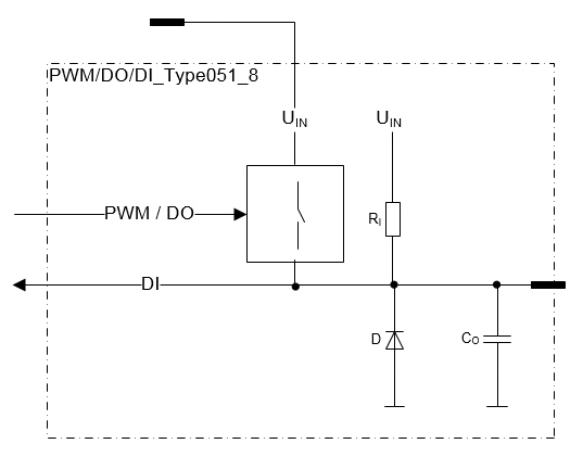
Output
This type of pin is a current sourcing output with a pull-up resistor
In other words, the pin connects the load to a positive supply voltage
The pull-up feature is for open load detection when the pin is used as an output.
These outputs have integrated protection features (overload, overcurrent)
These outputs are capable to generate pulse width modulated (PWM) output signals.
When used as an output, the input feature indicates the output FET's state
This kind of pin can be used with a step motor (for more information refer to the Programming and Libraries manual)
|
If you want to use current measuring, connect the other end of the load to the feedback pin.
|
|
It is recommended to use the function blocks in DigitalOutputDiagnostics library to protect and diagnose outputs when used as digital outputs. For more information, refer to Epec Programming and Libraries Manual. |
Input
This pin can be used as a digital input (DI)
This pin can be used also with NPN-type sensors – sensors with open collector/open drain.
A pin of this type can also be used as an input by using the output state monitoring feature.
In those cases the output functionality of the pin must be kept in off state.
It must be taken care in system design that the output unintentionally switching to on state causes no harm to the system.
It’s highly recommended to use closed loop connections when the output pin is used as input. By keeping this simple principle in your mind you will avoid many unknown problems later on.
Electrical characteristics
Symbol |
Parameter |
Conditions |
Min |
Max |
Units |
RO |
Output Resistance |
Output On |
|
0,2 |
Ω |
IO |
Output Current |
Output On |
0 |
3 |
A |
Io-lim |
Internal current limitation |
Output On (Note 1, 2) |
typ. 12 |
A |
|
fPWM |
PWM Frequency |
(Note 6) |
10 |
3000 |
Hz |
DutyPWM |
Duty Cycle |
(Note 3, 9) |
0 |
100,0 |
% |
ResPWM |
PWM Resolution |
(Note 8) |
|
0,1 |
% |
Digital status input |
|||||
RI |
Input Resistance |
Output Off; Referenced to Uin |
typ. 10 |
kΩ |
|
VI-level |
Input voltage level |
Output Off; Unconnected pin |
Uin |
V |
|
VIH |
Input High Voltage |
Output Off (Note 7) |
3,5 |
Uin |
V |
VIL |
Input Low Voltage |
Output Off |
-0,5 |
1,5 |
V |
fI |
Input frequency (digital input) |
50% duty cycle (Note 3, 4) |
|
1/ 2tC |
Hz |
tI |
Digital Status Input Pulse Width |
(Note 4, 5) |
> tC |
ms |
|
CO |
Output pin capacitance |
|
typ. 1 |
nF |
|
Note 1: Current limit for short circuit protection to protect cabling and to limit internal power dissipation.
Note 2: When the limit is exceeded, the output voltage circuit starts to limit the current by switching the output voltage. The switching does not effect the application software
Note 3: The duty cycle is defined as the percentage of digital ‘high’ to digital ‘low’ signals present during a PWM period.
Note 4: tC denotes the software cycle time.
Note 5: The pulse width must be greater that the software cycle time. For example with 50/50 pulse ratio, the pulse frequency is 1 / (2*pulse width)
Note 6: PWM capable outputs are divided into groups. All outputs in the same group share the same PWM frequency (default value 10 Hz). The groups are indicated with upper case characters in the pin table's Group column in section I/O List.
Note 7: Exceeding the max value might cause permanent damage.
Note 8: The PWM resolution is defined as a maximum number of pulses that you can pack into a PWM period.
Note 9: When the frequency increases, the actual duty cycle may be bigger than the value that has been set.