|
It is recommended to use the function blocks in DigitalOutputDiagnostics library to protect and diagnose outputs when used as digital outputs. For more information, refer to Epec Programming and Libraries Manual. |
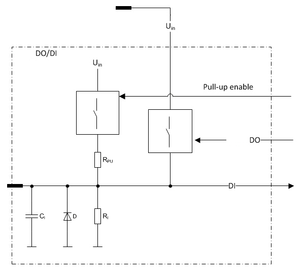
Possible pin modes:
Sourcing DO mode (pull-up)
Sourcing DO mode (pull-down)
DI mode (pull-up)
DI mode (pull-down)
This pin type is a current sourcing output with a pull-up selection
The pin connects the load to a positive supply voltage
The pull-up feature is for open load detection when the pin is used as an output
These outputs have a switching element called a smart FET. It has integrated features to protect itself and also the external pin, wiring and actuator.
When used as an output, the input feature indicates the output FET's state
|
It is recommended to use the function blocks in DigitalOutputDiagnostics library to protect and diagnose outputs when used as digital outputs. For more information, refer to Epec Programming and Libraries Manual. |
This pin can be used as a digital input (DI) by using the output state monitoring feature
In this case, the output (DO) functionality of the pin type must be kept OFF
This pin can be used also with NPN-type sensors – sensors with open collector/open drain
It’s highly recommended to use closed loop connections when the output pin is used as an input. By keeping this simple principle in your mind you will avoid many unknown problems later on
Electrical characteristics
|
Symbol |
Parameter |
Conditions |
Min |
Max |
Units |
|
VLevel |
Output voltage |
Output Off, Pull-up selected, Unconnected pin, Uin = 24 V VLevel = Uin/1,3 |
typ. 18,5 |
V |
|
|
Io |
Nominal Output Current |
Output On |
0 |
1 |
A |
|
Io-lim |
Internal current limitation |
Output On (Note 2, 6) |
typ. 12 |
A |
|
|
Digital status input |
|||||
|
RI |
Input Resistance |
Output Off, Pull-up resistor not selected, VI< Uin (referenced to GND) |
typ. 44 |
kΩ |
|
|
Output Off, Pull-up resistor selected, (referenced to Uin /1,3) |
typ. 8,1 |
kΩ |
|||
|
VIH |
High Voltage level |
Output Off (Note 3, 8) |
4,2 |
Uin |
V |
|
VIL |
Low Voltage level |
Output Off (Note 8) |
|
3,2 |
V |
|
VI-range |
Input voltage range |
(Note 7) |
-0,5 |
Uin |
V |
|
tI |
Digital Status Input |
(Note 1, 5)
|
> tC |
ms |
|
|
CI |
Input pin capacitance |
typ. 1 |
nF |
||
Note 1: tC denotes software cycle time.
Note 2: Current limit for short circuit protection to protect cabling and to limit internal power dissipation.
Note 3: Exceeding the max value might cause damage to input.
Note 4: The maximum output current depends on the load, PWM frequency and temperature.
Note 5: Pulse width must be greater that the software cycle time. For example with 50/50 pulse ratio, the pulse frequency is 1 / (2*pulse width)
Note 6: When the limit is exceeded, the output voltage circuit starts to limit the current by switching the output voltage. The switching does not affect the application software.
Note 7: Overload conditions
Note 8: Includes hysteresis. The input state is maintained until the second voltage limit is exceeded.