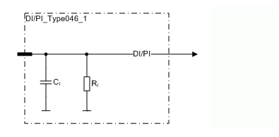
This kind of pins are digital inputs (DI) including a pulse counting (PI) feature.
This kind of pins have a pull-down resistor to ground
Pulse inputs can be used as a 1 or 2 channel pulse counter and they have a reset possibility. Possible software channels and pairs are listed in Epec Programming and Libraries Manual, section Programming 3724 > I/O > Pulse Inputs.
Electrical characteristics
|
Symbol |
Parameter |
Conditions |
Min |
Max |
Units |
|
RI |
Input Resistance |
Input high; Referenced to GND (Note 3) |
9,5 |
10,5 |
kΩ |
|
Input Low; Referenced to 1,4 V |
6,5 |
7,5 |
kΩ |
||
|
VI-level |
Input voltage level |
Unconnected pin |
typ. 1,4 |
V |
|
|
VIH |
Input High Voltage |
Overload conditions (Note 1) |
4,6 |
33 |
V |
|
VIL |
Input Low Voltage |
|
-0,5 |
4 |
V |
|
fI |
Input Frequency (frequency measurement and pulse counting) |
(Note 5, 6) |
|
20 |
kHz |
|
Input Frequency |
(Note 2, 4) |
|
1/ 2tC |
kHz |
|
|
tI |
Input Pulse Width |
|
1 |
10000 |
ms |
|
CI |
Input Capacitance |
|
typ. 1 |
nF |
|
Note 1: Exceeding the max value might cause damage to input.
Note 2: tC denotes the software cycle time in milliseconds.
Note 3: The input resistance is typically 10 kΩ, while input voltage is < 15 V. When input voltage increases over 15 V, the input resistance decreases in a non-linear function towards 6,5 kΩ.
Note 4: The pulse width must be greater that the software cycle time. For example with 50/50 pulse ratio, the pulse frequency is 1 / (2*pulse width)
Note 5: The maximum value can be reached with 50 % duty cycle.
Note 6: The maximum frequency sum for all the pins is 40 kHz.
Functional block diagram