![]()
Closed circuit loops are mandatory when using this pin.
Closed circuit loop means that the current from the control unit to the sensor must return to the same control unit, see the figures in section I/O Cabling.
|
|
Closed circuit loops are mandatory when using this pin. Closed circuit loop means that the current from the control unit to the sensor must return to the same control unit, see the figures in section I/O Cabling. |
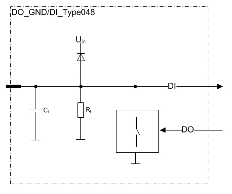
This kind of pins are current sinking outputs.
In other words, pins connect the load to the ground.
The application program can also simultaneously monitor the actual state of the pin.
This feature makes it possible to detect open loads and short circuits to the supply voltage.
|
It is recommended to use the function blocks in DigitalOutputDiagnostics library to protect and diagnose outputs when used as digital outputs. For more information, refer to Epec Programming and Libraries Manual. |
A pin of this type can also be used as an input by using the output state monitoring feature.
In those cases the output functionality of the pin must be kept in off state.
It must be taken care in system design that the output unintentionally switching to on state causes no harm to system.
Electrical characteristics
|
Symbol |
Parameter |
Conditions |
Min |
Max |
Units |
|
RO |
Output Resistance |
Output On |
|
0,12 |
Ω |
|
II |
Nominal Input Current |
Output On |
|
3 |
A |
|
IL |
Leakage Current |
Output Off |
typ. 3 |
mA |
|
|
Digital status input |
|||||
|
RI |
Input Resistance |
Output Off |
typ. 10 |
kΩ |
|
|
VIH |
Input High Voltage |
Output Off |
3,5 |
Uin |
V |
|
VIL |
Input Low Voltage |
Output Off |
-0,5 |
1,5 |
V |
|
fI |
Input frequency |
50% duty cycle (Note 1, 2) |
|
1/ 2tC |
Hz |
|
tI |
Input Pulse Width |
(Note 2, 3) |
> tC |
ms |
|
|
CI |
Input Pin Capacitance |
|
typ. 1 |
nF |
|
Note 1: The duty cycle is defined as the percentage of digital ‘high’ to digital ‘low’ signals present during a PWM period.
Note 2: tC denotes the software cycle time.
Note 3: The pulse width must be greater that the software cycle time. For example with 50/50 pulse ratio, the pulse frequency is 1 / (2*pulse width)
Functional block diagram