![]()
If you want to use current measuring, connect the other end of the load to the feedback pin.
These pins are current sourcing outputs.
In other words, pin connects the load to positive supply voltage.
The application program can also simultaneously monitor the actual state of the pin.
This feature makes it possible to detect short circuits to the ground and short circuits to the power supply.
Open loads can not be detected because the internal load resistor is connected to the ground.
These kind of outputs are also capable to generate pulse width modulated (PWM) output signals.
This feature is useful when driving proportionally controlled loads, e.g. proportional hydraulic valves.
PWM frequencies can be configured under software control in groups of outputs.
The setting is done by a PWM channel, setting the frequency of one channel sets also the frequencies of all the other channels in the same group.
The groups are indicated with upper case characters in the pin table's Group column in section I/O List).
These outputs have integrated protection features (overload, overcurrent)
This kind of pin can be used with a step motor (for more information refer to the Programming and Libraries manual)
|
|
If you want to use current measuring, connect the other end of the load to the feedback pin.
|
|
It is recommended to use the function blocks in DigitalOutputDiagnostics library to protect and diagnose outputs when used as digital outputs. For more information, refer to Epec Programming and Libraries Manual. |
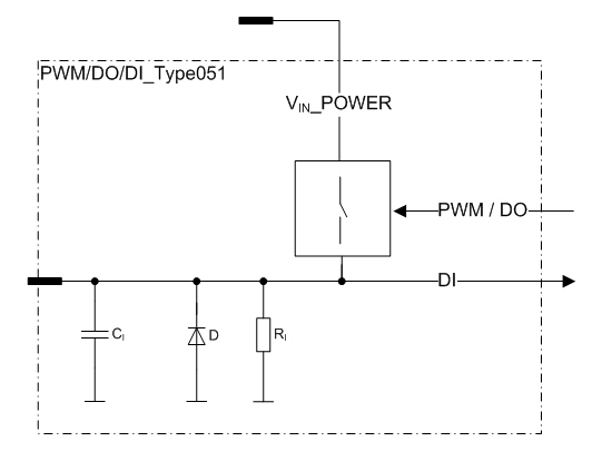
This pin can be used as a digital input (DI)
A pin of this type can also be used as an input by using the output state monitoring feature.
In this case, the output functionality of the pin must be kept in the off state.
|
Closed circuit loops are mandatory when you are using DO or PWM pin as an input. Closed circuit loop means that the current from the control unit to the sensor must return to the same control unit, see the figures in section I/O Cabling. |
|
Symbol |
Parameter |
Conditions |
Min |
Max |
Units |
|
RO |
Output Resistance |
Output On |
|
0,2 |
Ω |
|
IO |
Output Current |
Output On |
0 |
3 |
A |
|
Io-lim |
Internal current limitation |
Output On (Note 2, 3) |
typ. 12 |
A |
|
|
fPWM |
PWM Frequency |
(Note 1) |
10 |
3000 |
Hz |
|
DutyPWM |
Duty Cycle |
(Note 4, 9) |
0 to 100,0 |
% |
|
|
ResPWM |
PWM Resolution |
(Note 1, 8) |
0,1 |
% |
|
|
Digital status input |
|||||
|
RI |
Input Resistance |
Output Off; Referenced to GND |
typ. 10 |
kΩ |
|
|
VIH |
Input High Voltage |
Output Off (Note 7) |
3,5 |
Uin |
V |
|
VIL |
Input Low Voltage |
Output Off |
-0,5 |
1,5 |
V |
|
fI |
Input frequency (digital input) |
50% duty cycle (Note 4, 5) |
|
1/ 2tC |
Hz |
|
tI |
Digital Status Input Pulse Width |
(Note 5, 6) |
> tC |
ms |
|
|
CI |
Input pin capacitance |
|
typ. 1 |
nF |
|
Note 1: PWM capable outputs are divided into groups. All outputs in the same group share the same PWM frequency (default value 10 Hz). The groups are indicated with upper case characters in the pin table's Group column in section I/O List.
Note 2: Current limit for short circuit protection to protect cabling and to limit internal power dissipation.
Note 3: When the limit is exceeded, the output voltage circuit starts to limit the current by switching the output voltage. The switching does not effect the application software.
Note 4: The duty cycle is defined as the percentage of digital ‘high’ to digital ‘low’ signals present during a PWM period.
Note 5: tC denotes the software cycle time.
Note 6: The pulse width must be greater that the software cycle time. For example with 50/50 pulse ratio, the pulse frequency is 1 / (2*pulse width)
Note 7: Exceeding the max value might cause permanent damage.
Note 8: The PWM resolution is defined as a maximum number of pulses that you can pack into a PWM period.
Note 9: When the frequency increases, the actual duty cycle may be bigger than the value that has been set.
Functional block diagram