|
It is recommended to use the function blocks in DigitalOutputDiagnostics library to protect and diagnose outputs when used as digital outputs. For more information, refer to Epec Programming and Libraries Manual. |
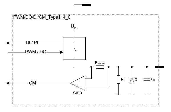
Output (PWM/DO)
This type of pin is a current sourcing output with a pull-down resistor
This pin includes a current measurement feature (the pin connects the load to a positive supply voltage through the shunt resistors)
These outputs have a switching element called a smart FET. It has integrated features to protect itself and also the external pin, wiring and actuator.
These outputs are capable of generating pulse width modulated (PWM) output signals.
When used as an output, the status feature indicates the output FET's state
|
It is recommended to use the function blocks in DigitalOutputDiagnostics library to protect and diagnose outputs when used as digital outputs. For more information, refer to Epec Programming and Libraries Manual. |
Current feedback
Input (DI)
A pin of this type can be used as digital input by using the output state monitoring feature.
In those cases the output functionality of the pin must be kept in off state.
This pin can be used also with PNP-type sensors
It must be taken care in system design that the output unintentionally switching to on state causes no harm to the system.
It’s highly recommended to use closed loop connections when the output pin is used as an input. By keeping this simple principle in your mind you will avoid many unknown problems later on.
Electrical characteristics
Symbol |
Parameter |
Conditions |
Min |
Max |
Units |
RShunt |
Shunt resistance |
|
typ. 15 |
mΩ |
|
Io-range |
Nominal Current Measuring Range |
|
0 |
3 |
A |
Io |
Nominal Output Current |
Output On |
0 |
3 |
A |
fPWM |
PWM Frequency |
(Note 1) |
10 |
3000 |
Hz |
DutyPWM |
PWM |
(Note 2, 8) |
0 to 100 |
% |
|
ResPWM |
PWM Resolution |
(Note 3) |
0,1 |
% |
|
Digital status input |
|||||
RI |
Input Resistance |
Output Off; Referenced to GND |
typ. 10 |
kΩ |
|
VIH |
Input High Voltage |
Output Off (Note 6) |
4,1 |
Uin |
V |
VIL |
Input Low Voltage |
Output Off |
-0,5 |
3,3 |
V |
fI |
Input frequency (digital input) |
50% duty cycle (Note 3, 4) |
1/ 2tC |
Hz |
|
tI |
Digital Status Input Pulse Width |
(Note 2, 4, 5) |
> tC |
ms |
|
CO |
Output pin capacitance |
|
typ. 1 |
nF |
|
Note 1: Frequency of a (PWM) Pulse
Width Modulation
is = 1 / Period
Note 2: The duty cycle is defined as the percentage
of digital ‘high’ to digital ‘low’ signals present during a PWM period.
Note 3: The
PWM resolution is defined as the maximum number of pulses that you can
pack into a PWM period.
Note 4: tC denotes software cycle time.
Note 5: The pulse width must be greater that the software cycle time. For example with 50/50 pulse ratio, the pulse frequency is 1 / (2*pulse width)
Note 6: Exceeding the max value might cause permanent damage.